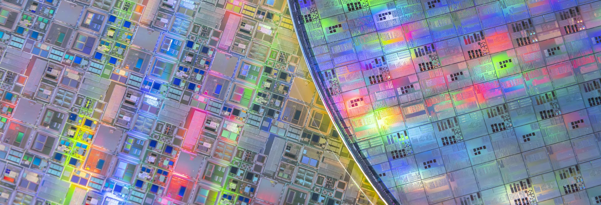
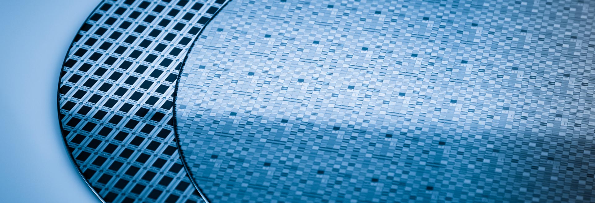

Semiconductor
Advanced Engineered Materials for Semiconductors
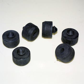
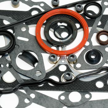
Sophisticated fabrication and automated test equipment streamlines quality assurance during production and requires levels of precision that can only be achieved with high performance engineered material solutions. Pure, stable, and ultraclean materials help maintain a contaminant-free production and test environment required for high quality, reliable semiconductors. Vibration mitigation, environmental sealing, thermal insulation, electrical isolation, high temperature bonding, FFKM o-rings, and EMI and RF shielding protect semiconductors during fabrication and testing to ensure accuracy and increase semiconductor chip yield.

Lower Total Cost of Ownership
Integrated solutions minimize or remove waste, maintenance costs, and downtime.
Global Resources, Regional Support
Respond quickly to geopolitical changes, strategy shifts in region sourcing, near-shoring or global manufacturing moves with Boyd’s supply chain flexibility and replicated, scalable, global manufacturing.
Accelerate Time to Market
Customer-first service with market leading speed and responsiveness combined with decades of semiconductor design expertise and robust, proprietary modeling tools enable Boyd to iterate designs quickly and accelerate speed to market.
Related Products & Resources
Have questions? We’re ready to help!